Promising First Results from Scanning Tunneling Microscope
Promising First Results from Low Temperature Scanning Tunneling Microscope
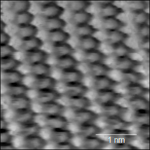
A team of CMU physicists has succeeded in producing an atomic scale image of Tungsten Ditelluride, one of the most tantalizing materials of the future.
Tungsten Ditelluride (WTe2) is mostly an insulator, not generally capable of conducting electricity. However, at low temperatures the material can conduct electricity in a robust way insensitive to the presence of any defects. This makes WTe2 a topological insulator, with properties that will likely spur technological innovations in science and computing that are just beginning to be imagined. The first step in unlocking this enormous potential is to prepare a sample of WTe2 and study its electronic properties at low temperature.
Easier said than done. A multitude of challenges remain, not least of which is the fact that WTe2 is sensitive to air. How does one prepare a pure sample? If different stages of this need to be done in different labs, how does one transport the material from one place to another without destroying its purity? How does one study its properties at low temperature?
Enter the team led by Professors Randall Feenstra and Ben Hunt, working with postdoc Felix Lupke, grad student Dacen Waters, and undergrads Nicolas Iskos and Nick Speeney. They first obtained an NSF grant for a low temperature scanning tunneling microscope (STM) that can characterize materials such as WTe2. Then they placed a flake of WTe2, supported by a small piece of graphite, on silicon wafer decorated with a gold pattern.
To prevent contamination, the sample had to be placed in a glove box containing no water or oxygen. Once constructed in Hunt’s lab on the 7th floor of Wean Hall, sample and wafer had to be transported down six stories in an inert gas suitcase before being placed within the STM. The STM tip was able to locate the sample by sensing the conductance of the underlying gold pattern. The result is the image shown above, an atomic scale view of a material with exciting technological potential.
This is only the beginning; the team will continue to focus on spectroscopic measurements using the STM in an effort to reveal the topological nature of the WTe2 electronic states.