Feenstra Wins Davisson-Germer Prize
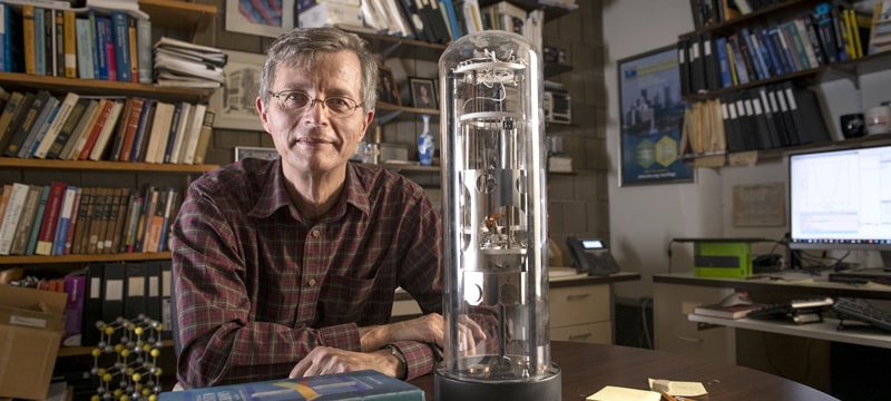
CMU Physics Professor Randall Feenstra has been named the winner of the 2019 Davisson-Germer Prize in Atomic or Surface Physics from the American Physical Society. The award, which is only given to surface physicists every two years, recognizes Feenstra’s “pioneering developments of the techniques and concepts of spectroscopic scanning tunneling microscopy."
Those pioneering developments began in Yorktown Heights, NY, 1982. Dr. Feenstra was a freshly-minted PhD studying point defects in semi-conductors for IBM. “At that time, I honestly viewed the IBM Lab as being the center of the universe,” said Feenstra. “Hundreds of scientists running around, just doing the research that they wanted to do, with no immediate application to the company, and seeing where that took them.”
The year before, Gerd Binnig and Heinrich Rohrer had invented an incredible new device at the IBM lab in Zürich, Switzerland: the Scanning Tunneling Microscope. In the STM, a ultra-sharp probe tip is positioned about one nanometer – one hundredthousandth of the diamater of a hair – from the surface of the sample under study, then scanned across that surface. Experiments are performed in ultra-high vacuum, so electrons can only travel between the tip and the sample in a quantum mechanical process by "tunneling" through that narrow vacuum gap. Voltage is applied between the probe-tip and the sample, creating a tunneling current between them. This current is dependent on the separation between the probe-tip and the sample surface, so by scanning the tip across the surface, one could build up an image of the morphology (i.e. raised and lowered areas) of the surface – and that at a resolution which for the first time made atoms on the surface directly visible. The STM is so sensitive to the minutest differences in morphology along the sample’s surface that it can reveal the position of individual atoms! Never before had there been a device capable of imaging the surface of a substance at the atomic level. Feenstra found this breakthrough new technology intriguing. While in Europe for a conference on Semiconductor Physics, he joined a group of IBM scientists on a trip to Zürich to see the STM for himself.
“At dinner that night, one of the managers of IBM New York said we should build one,” remembers Feenstra. “They were looking for a young person, so I volunteered. I needed a project, and it was the field I wanted to go into.” So began Feenstra’s career in surface physics: he built an STM for the IBM lab in Yorktown Heights.
“The facilities at IBM were simply the best available,” said Feenstra. “I still have dreams about raiding the stock room for ultra-high-vacuum equipment.”
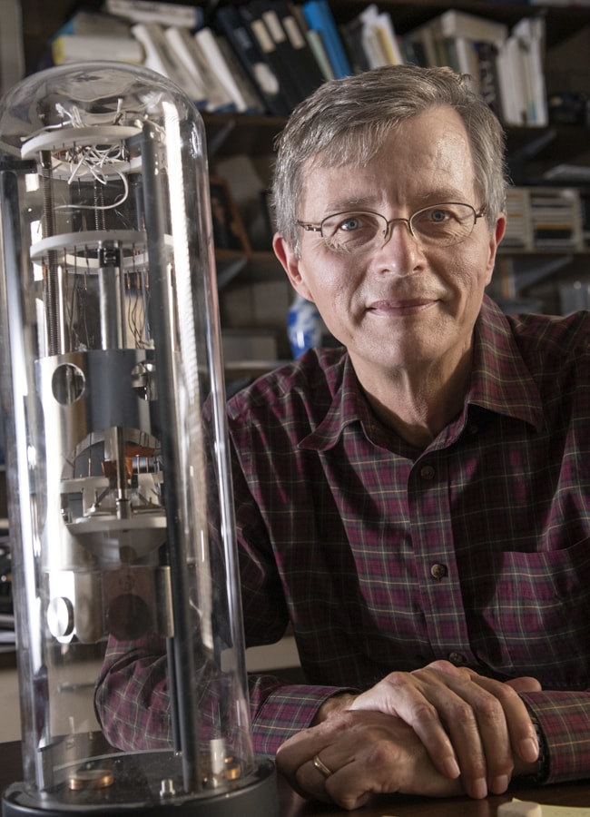
Joining the CMU Physics faculty in 1995, Feenstra brought the STM with him and continued to strengthen and develop new techniques in spectroscopic scanning tunneling microscopy.
“CMU was the first Physics department I’d ever been a part of, and I’m very grateful for all the support that the various department heads have given me,” Feenstra said.
Feenstra did more than just reconstruct Binnig and Rohrer’s invention, however. He realized the device could be used to specifically yield spectroscopic measurements. In this mode, the probe-tip is positioned at a particular location on the surface, e.g. over an atom of interest, and then the voltage between the tip and surface is varied. The precise magnitude of the voltage can access different electronic states of the sample, located at different energies. If one then plots the current vs. voltage, a spectrum is obtained which reveals information about the electronic states at specific energies and with specific spatial locations on the surface.
Feenstra made a number of early contributions in devising solutions to common problems found in the methods of data acquisition and analysis for spectroscopic measurements with the STM. One such problem is that the magnitude of the current sent through the STM can vary widely as the voltage is varied, and surface physicists want to record all of these current magnitudes. However, too strong a current can damage the probe-tip or the sample surface in the STM, while too weak a current is limited by electrical noise which muddies the data. Recording only measurements between these two extremes would not provide enough significant data. Feenstra discovered that varying the tip-sample separation – either by performing measurements at several different tip-sample separations, or by continuously varying the tip-sample separation during the measurement – achieves a high dynamic range in the measurement. This observation led to the development of various methods to standardize variations in tip-sample separation, thus yielding spectra that nicely characterize the electronic properties of the surface.
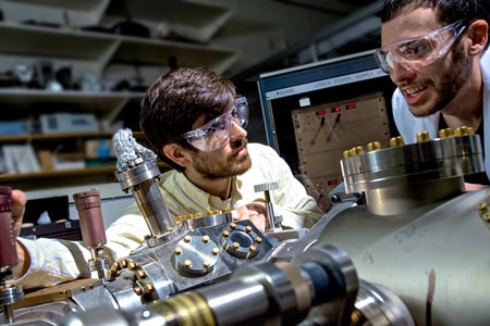 Post-doctoral researcher Sergio de la Barrera and graduate student Dacen Waters make adjustments on an ultra-high vacuum system in Feenstra's lab, used to probe electronic states.
Another problem Feenstra faced occurred specifically for semiconductor samples that have a band gap – an energy region where no states exist in the bulk material. This energy gap remains even when surface states are considered, with a consequence being that part of the voltage applied between the tip and the sample is dropped within the semiconductor itself. This phenomena is known as "band bending" in the semiconductor; it is the basis for operation of all semiconductor devices. However, within the context of STM, this type of “tip-induced band bending” results in significant uncertainty in the interpretation of the spectra: In the absence of this effect, the energies of states correspond directly to applied voltages between the sample and the tip, whereas with the effect, these energies all shift relative to the applied voltages (and the shift depends on the magnitude of the voltage).
In order to enable a quantitative evaluation of tip-induced band bending, Feenstra developed a set of computer programs that fully solved this electrostatic problem, including computation of tunnel currents. Feenstra’s codes have been applied to various problems involving measured STM spectroscopic data, and are now used world-wide by researchers to evaluate the effects of tip-induced band bending for their own experiments.
For these accomplishments, along with his many other contributions to advancing STM technology, Feenstra will be officially awarded the prestigious Davisson-Germer Prize at the 2019 March Meeting of the American Physical Society.
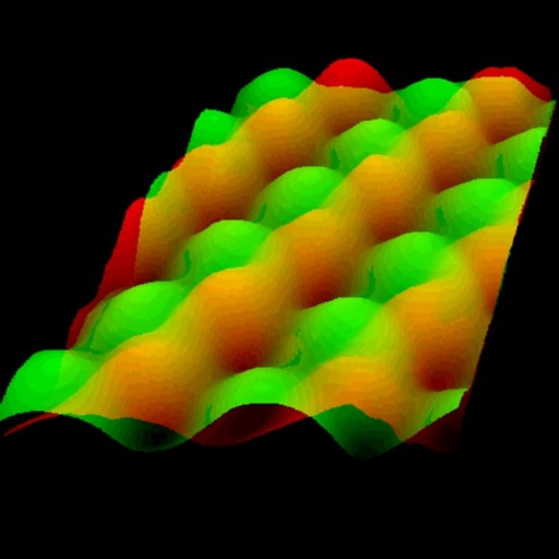 STM image of the (110) surface of a gallium arsenide crystal. Gallium atoms (empty states) are pictured in green, and arsenic atoms (filled states) are shown in red. Spectroscopic imaging, in which the sample-tip voltage is varied between images, permits the discrimination between the types of atoms on the surface.