Imaging of devices in operando
Many of the memory devices rely on motion of ions or changes in the phase of the functional material to store information. The best way to understand these processes is to directly image the changes occurring during device operation. This means powering the devices up inside the electron microscope.
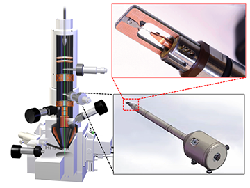
Schematics of the in situ TEM experiment and the TEM sample on the biasing holder.
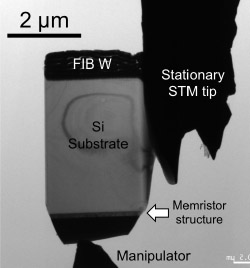
Extension and contraction of planar Wadsley faults in Pt/TiO2/Pt device during resistive switching.
Much can be learned about function of devices by imaging the temperature distribution. In switching devices, current spontaneously constricts forming a small filament. This causes local temperature increase allowing for measuring the filament size as a function of bias. We are using scanning probe microscopy to map out the temperature.
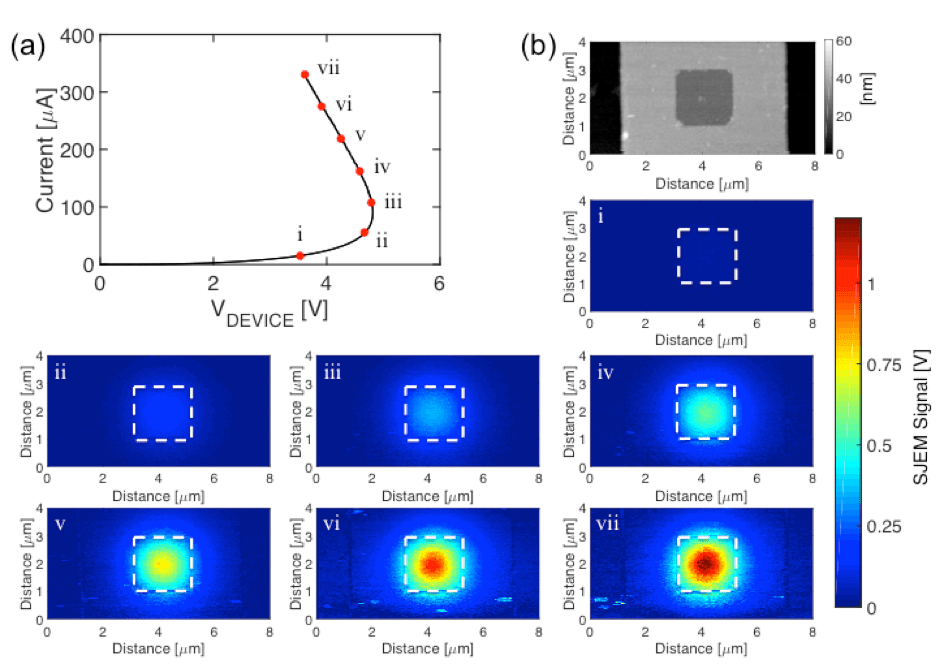
Scanning Joule Expansion Microscopy maps of the selector TiN/TiOx/TiN device.
Collaborations:
![]()
![]()